Revolutionizing Nuclear Safety: Real-time 3D Imaging Technique Unveils Material Failures
2025-08-27
Author: Ming
A Breakthrough in Nuclear Reactor Monitoring
Researchers at MIT have made a groundbreaking advancement, developing a real-time, 3D imaging technique that captures corrosion, cracking, and other material failures within nuclear reactors. This innovative approach promises to enhance the safety and longevity of nuclear reactors, paving the way for safer electricity generation and naval propulsion.
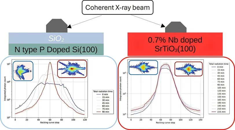
Harnessing High-Powered X-Rays for a New Era of Insight
In their experiments, the team harnessed the power of high-intensity X-rays to replicate neutron interactions with materials found inside a reactor. They discovered that introducing a silicon dioxide buffer between materials dramatically improved sample stability, allowing for real-time observation of failure processes.
Understanding Failures Like Never Before
By generating 3D images of material structures as they fail, these innovative techniques could lead to the creation of more resilient materials capable of enduring the harsh conditions within nuclear reactors. Ericmoore Jossou, a leading professor in nuclear science at MIT, expressed the technique's potential, stating it could significantly extend reactor lifespans and improve material performance.
Unprecedented Nanoscale Measurements
According to lead author David Simonne, this method allows for unprecedented nanoscale resolution measurements during corrosion processes—critical for advancing nuclear science and engineering. Traditionally, researchers could only analyze failed materials post-fact, but now they can observe failure mechanisms in real time.
Crafting Ideal Samples for Success
The journey to this discovery involved meticulous preparation of nickel samples, essential for the alloys commonly used in advanced reactors. The team faced challenges when heating the nickel, leading to unwanted chemical reactions with its substrate. After numerous trials, they successfully applied a silicon dioxide layer, preventing such reactions and stabilizing their samples.
Unlocking New Dimensions of Material Science
Not only does this technique offer insight into material failures, but it also allows researchers to manipulate strain levels in materials, which could drastically impact microelectronics development. Engineers can tune the strain of crystals during fabrication, enhancing their electrical and optical properties.
Future Horizons in Material Research
Looking ahead, the researchers aim to explore how this technique can be applied to more complex materials, such as steel and various metal alloys used across nuclear and aerospace industries. They are particularly interested in how variations in the silicon dioxide layer can further influence strain control.
A Significant Step Forward for Material Science
As noted by Edwin Fohtung from Rensselaer Polytechnic Institute, this discovery is vital for understanding how nanoscale materials react to radiation—a crucial aspect for the future of energy technology, microelectronics, and quantum materials. The researchers' findings underscore the importance of substrate selection in managing strain during focused X-ray investigations.


 Brasil (PT)
 Canada (EN)
 Chile (ES)
 Česko (CS)
 대한민국 (KO)
 España (ES)
 France (FR)
 Hong Kong (EN)
 Italia (IT)
 日本 (JA)
 Magyarország (HU)
 Norge (NO)
 Polska (PL)
 Schweiz (DE)
 Singapore (EN)
 Sverige (SV)
 Suomi (FI)
 Türkiye (TR)
 الإمارات العربية المتحدة (AR)