Revolutionary Single Transistor Breakthrough Could Transform Neuromorphic AI Chips Forever!
2025-03-31
Author: Nur
In an astonishing breakthrough, researchers from the National University of Singapore (NUS) have harnessed a phenomenon typically seen as a failure mode in traditional silicon transistors to develop a single transistor capable of simplifying neuromorphic AI chip designs dramatically. This innovation promises to revolutionize how artificial neural networks function, opening the door to more efficient and powerful computing systems!
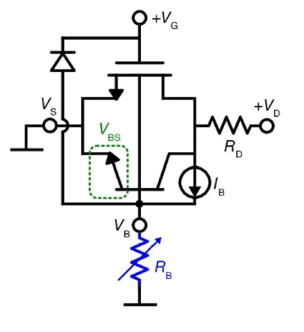
Traditionally, implementing neurons and synapses in neuromorphic chips requires a staggering 18 transistors for each neuron and 6 for each synapse. However, this cutting-edge research team has discovered a way to emulate the essential electronic behaviors of neurons and synapses by controlling the resistance of the bulk terminal in a metal-oxide-semiconductor field-effect transistor (MOSFET) to invoke a physical phenomenon known as impact ionization.
Operating at the verge of "punch-through" conditions while adjusting the bulk resistance creates a current spike reminiscent of the activity seen in biological neurons. This technique is groundbreaking! The phenomenon, generally regarded as a failure mechanism, has been reigned in to serve a revolutionary purpose: the creation of a Neuro-Synaptic Random Access Memory (NS-RAM) cell.
By fine-tuning the bulk resistance to specific values, the new transistor can also mimic the behavior of electronic synapses, enabled to retain charge in the gate oxide and maintain its resistance over time. The implications are profound: this single transistor can switch between acting as a neuron or synapse, depending on the desired setting.
In "neuron mode," the two-transistor cell could effectively reproduce leaky integrate-and-fire neural behavior and show adaptive frequency bursting with remarkable performance metrics — such as a high switching slope of below 10 mV/dec, a dynamic range exceeding 1000, and an endurance of over 10 million cycles, all with exceptional energy efficiency down to just 415 picojoules per cubic micron.
Switching gears to "synapse mode," the transistor can store at least six distinct synaptic weights, maintaining stability and durability over an impressive 100,000 cycles. This adaptability signifies a monumental leap in the capabilities of artificial neural networks, as every network can involve millions of electronic neurons and synapses!
Professor Mario Lanza and his team emphasize that this technology leverages commercial CMOS (complementary metal-oxide-semiconductor) processes, commonly used in modern processors and memory chips. This compatibility ensures that the innovation is not only scalable and reliable but seamlessly integrates into existing semiconductor fabrication workflows.
"Once the operating mechanism was discovered, it was simply a matter of microelectronic design," Lanza asserted, pointing to the straightforwardness of adapting established technologies.
As the digital landscape evolves, the extraordinary potential of this NS-RAM cell suggests that power-hungry traditional computing could soon be an artifact of the past. With the potential to process vast amounts of information more efficiently, this breakthrough could pave the way for a new era of energy-efficient and highly capable artificial intelligence platforms. The questions of "How soon will we see practical applications?" and "What changes will this bring to everyday technology?" linger in the air as excitement builds around this groundbreaking research.
Stay tuned as we continue to cover developments in neuromorphic computing that promise to reshape the future of technology!


 Brasil (PT)
 Canada (EN)
 Chile (ES)
 Česko (CS)
 대한민국 (KO)
 España (ES)
 France (FR)
 Hong Kong (EN)
 Italia (IT)
 日本 (JA)
 Magyarország (HU)
 Norge (NO)
 Polska (PL)
 Schweiz (DE)
 Singapore (EN)
 Sverige (SV)
 Suomi (FI)
 Türkiye (TR)
 الإمارات العربية المتحدة (AR)