Revolutionary Broadband Photodetector Material: The Future of Smart Sensors
2025-09-24
Author: Sarah
A Breakthrough in Sensor Technology
In an exciting development, a research team from South Korea has unveiled a cutting-edge sensor material that can detect multiple light wavelengths—transforming the landscape of smart technology.
Meet the Game-Changing Broadband Photodetector
Led by Dr. Wooseok Song from the Korea Research Institute of Chemical Technology alongside Professor Dae Ho Yoon from Sungkyunkwan University, this innovative broadband photodetector material significantly outperforms existing commercial alternatives. With the ability to sense a broader range of wavelengths and manufactured on a 6-inch wafer-scale, this breakthrough is both efficient and cost-effective.
From Multiple Sensors to One Integrated Solution
Typically, different types of sensors are needed for various wavelength ranges—think visible light, near-infrared, mid-infrared, and long-wave infrared—especially in applications like autonomous vehicles or military drones where multiple sensors are cumbersome. The new broadband photodetector combines all these capabilities into a single unit, meeting the needs for efficient recognition, distance measurement, and night-time detection.
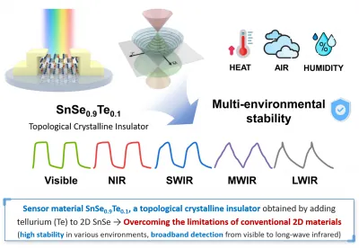
A Material That Defies Conventional Limitations
Utilizing a topological crystalline insulator (SnSe₀.₉Te₀.₁), derived from the 2D semiconductor tin selenide, the material showcases excellent stability and sensitivity. Unlike traditional semiconductors that struggle to detect low-energy photons, the TCI's unique structure allows electrons to move freely, enabling precise detection of faint thermal radiation, like that emitted from human fingers.
Broader Detection and Enhanced Stability
The new material boasts an unprecedented detection range of approximately 8 times wider (0.5-9.6 μm) than that of conventional 2D semiconductors (0.4-1.2 μm). Not only is it lightweight and thin, but it also withstands extreme conditions, from high humidity to underwater environments.
Cost-Effective and Scalable Manufacturing
Perhaps even more revolutionary is the simplified fabrication process. Traditional techniques requiring costly materials like ultra-high vacuum equipment have been replaced with a more economical solution-based thermal decomposition method, allowing for uniform production on compact wafers compatible with existing semiconductor processes.
A Bright Future Ahead for Smart Technology
The research team is already pushing for further advancements, aiming for 8-inch wafers and complete sensor module integration. Dr. Song anticipates applications spanning from military drones and autonomous vehicles to smartwatches and home security systems.
A Leap Towards Domestic Innovation
KRICT President Young-Kuk Lee emphasizes the significance of this breakthrough, stating it could replace expensive imported sensors with high-performance, domestically produced alternatives.
Published in Leading Scientific Journal
This revolutionary study was recently published in ACS Nano, a prestigious journal, marking a pivotal moment in sensor technology.
Conclusion
This innovative research not only signifies a monumental leap in sensor capabilities but also positions South Korea as a leader in the field of advanced materials—potentially changing how smart devices operate today.


 Brasil (PT)
 Canada (EN)
 Chile (ES)
 Česko (CS)
 대한민국 (KO)
 España (ES)
 France (FR)
 Hong Kong (EN)
 Italia (IT)
 日本 (JA)
 Magyarország (HU)
 Norge (NO)
 Polska (PL)
 Schweiz (DE)
 Singapore (EN)
 Sverige (SV)
 Suomi (FI)
 Türkiye (TR)
 الإمارات العربية المتحدة (AR)