Revolutionary 3D Photonic-Electronic Technology Set to Transform AI Hardware: Could This Be the Future of Computing?
2025-03-23
Author: Wei
Introduction
Artificial intelligence (AI) is at the forefront of technological advancement, but a significant barrier has hindered its progress: the inefficiencies in energy consumption and data transfer bottlenecks. A groundbreaking new study from researchers at Columbia Engineering introduces a game-changing solution: a cutting-edge 3D photonic-electronic platform designed to enhance energy efficiency and bandwidth, heralding the dawn of next-generation AI hardware.
Background on the Study
In a paper titled "3D Photonics for Ultra-Low Energy, High Bandwidth-Density Chip Data Links," which recently appeared in Nature Photonics, Dr. Keren Bergman, the Charles Batchelor Professor of Electrical Engineering at Columbia, sheds light on this innovative approach. The research reveals a revolutionary integration of photonics with state-of-the-art complementary metal-oxide-semiconductor (CMOS) electronics, tackling longstanding challenges that have impeded the rapid evolution of AI technologies.
"In our work, we unveil a technology that can transfer massive data volumes with remarkably low energy consumption," Dr. Bergman stated. "This breakthrough dismantles the historic energy barriers that have constrained the movement of data in conventional computer and AI systems."
A Groundbreaking Leap in Data Communication
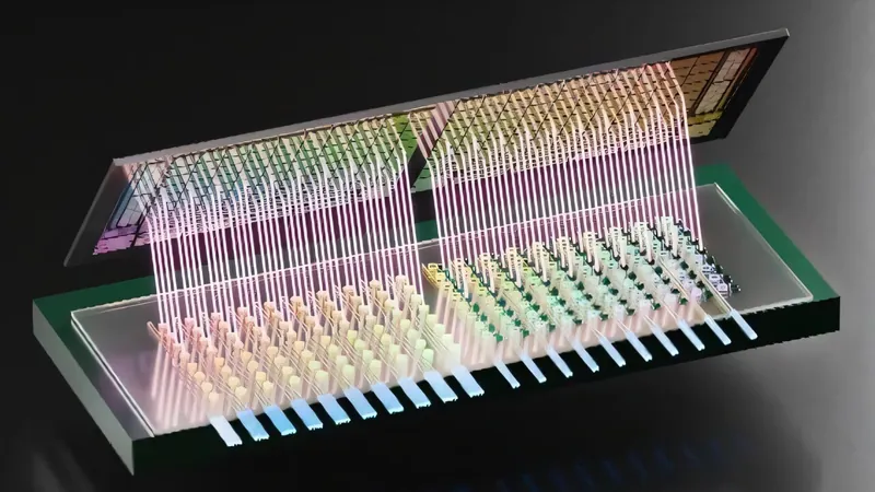
In collaboration with Dr. Alyosha Christopher Molnar from Cornell University, the Columbia team has engineered a 3D-integrated photonic-electronic chip that includes an impressive array of 80 photonic transmitters and receivers within a compact footprint. This revolutionary platform supports an astounding bandwidth of 800 Gb/s while consuming only 120 femtojoules per bit of data—demonstrating a bandwidth density of 5.3 Tb/s/mm², far surpassing current performance metrics.
What sets this chip apart is its affordability; it integrates photonic devices seamlessly with CMOS electronic circuits and employs components that can be produced in standard commercial foundries. This opens the door for widespread adoption across various industries, potentially changing the landscape of computing.
Unlocking the Future of AI and Beyond
This innovative technology redefines data transmission among compute nodes, eliminating traditional energy efficiency and scalability issues. By merging photonic and electronic chips in a 3D configuration, this platform achieves unparalleled energy efficiency and throughput, liberating AI systems from previous spatial and temporal constraints.
As a result, we could witness an extraordinary surge in performance across diverse applications, from sprawling AI models to real-time data analytics in autonomous vehicles. But the potential doesn't stop with AI; this methodological advancement could also revolutionize high-performance computing, telecommunications, and disaggregated memory systems.
With energy-efficient, high-speed computing infrastructure becoming a reality, we may very well be on the brink of a technological renaissance that reshapes our digital universe. Keep your eyes peeled—this breakthrough might just be the key to unlocking transformative innovations we cannot yet even imagine!


 Brasil (PT)
 Canada (EN)
 Chile (ES)
 Česko (CS)
 대한민국 (KO)
 España (ES)
 France (FR)
 Hong Kong (EN)
 Italia (IT)
 日本 (JA)
 Magyarország (HU)
 Norge (NO)
 Polska (PL)
 Schweiz (DE)
 Singapore (EN)
 Sverige (SV)
 Suomi (FI)
 Türkiye (TR)
 الإمارات العربية المتحدة (AR)