Groundbreaking Research Unveils How Layering and Twisting Transform Graphene's Optical Conductivity
2024-11-07
Author: Daniel
Introduction
Graphene, renowned for its incredible properties—being stronger than steel, lighter than aluminum, and more electrically conductive than copper—has emerged as a game-changer in the realm of nanomaterials. This single layer of carbon atoms, arranged in a honeycomb lattice, has captured the attention of physicists and engineers alike, paving paths for advanced technological applications.
Research Overview
In a landmark study published in Nano Letters, researchers from the Florida State University Department of Physics and the National High Magnetic Field Laboratory have uncovered how the physical manipulation of graphene—including layering and twisting—affects its optical properties and conductivity. Spearheaded by Assistant Professor Guangxin Ni and his team, the research could redefine our understanding of graphene's capabilities.
Twisted Bilayer Graphene
The researchers primarily focused on twisted bilayer graphene, a fascinating form of graphene where two layers are rotated relative to each other. Their findings revealed that the conductivity of this material remains largely unaffected by traditional physical or chemical manipulations—it largely hinges on the intricate geometric structure arising from these interlayer twists. This insight opens the door to further investigations into how temperature changes and varying frequencies can influence graphene's properties.
Imaging Techniques
Graduate research assistant Ty Wilson explained the impetus behind this research: "We sought to clarify the optical characteristics of twisted bilayer graphene, particularly looking at different twisting angles. Previous imaging efforts had not made such comparisons."
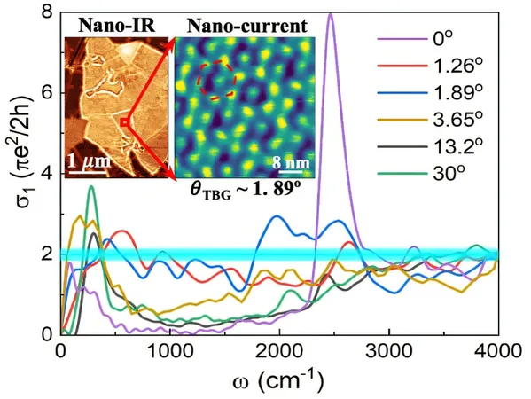
Utilizing advanced imaging techniques, the team examined plasmonic behaviors—small waves of energy generated by the collective movement of electrons—across regions of twisted bilayer graphene. They employed a cutting-edge scanning near-field optical microscope, which dazzlingly illuminated the sample with infrared light, allowing them to capture detailed nanoscale images.
"We used a specialized needle to enhance light-matter interactions, enabling us to visualize these plasmonic waves," Wilson elaborated, emphasizing the innovative approach their technology provided.
Grain Boundaries
The study also explored the material's grain boundaries—defects in the crystalline structure—allowing researchers to differentiate regions within the twisted bilayer graphene. These regions—where the carbon layers twist at unique angles—combined with a layer of hexagonal boron nitride beneath them, resulted in what scientists describe as a double-moiré pattern—a fascinating interplay of geometric designs.
Key Findings
As the team delved deeper, they discovered that the optical conductivity of the twisted bilayer graphene varied little with twist angles under two degrees, even under conditions of chemical doping and fluctuations in infrared light frequencies. This finding suggests that the opto-electronic properties of this super-moiré material rely more on its structural configuration than on external variables—an insight that could spur innovations in graphene-based technologies.
Implications of the Research
Lewandowski, another co-author of the study, shared his excitement about the research's implications: "The potential for multilayer moiré systems in developing materials with customizable optical properties is vast."
Furthermore, the measurement techniques implemented by Ni's group allow a thorough exploration of the local optical responses in two-dimensional systems, complementing existing methodologies in 2D materials research. The study suggests a remarkable capability for 2D systems to achieve nearly uniform optical responses across a broad range of light frequencies, all without needing active electronic intervention.
Conclusion
This research highlights the crucial role of geometric characteristics in double-moiré lattices and has significant implications for how nanomaterials react to various manipulations. The understanding gained from this work could aid scientists in engineering materials with highly desirable optical properties, leading to groundbreaking advancements in moiré optoelectronics, thermal imaging technologies, and improvements in optical switching for computer processors.
In a world racing towards technological innovation, this pivotal research presents a roadmap for continuous exploration of nano-optical phenomena, promising a future where graphene can be harnessed for even more powerful applications ensuring a smarter technological landscape.

 Brasil (PT)
 Canada (EN)
 Chile (ES)
 España (ES)
 France (FR)
 Hong Kong (EN)
 Italia (IT)
 日本 (JA)
 Magyarország (HU)
 Norge (NO)
 Polska (PL)
 Schweiz (DE)
 Singapore (EN)
 Sverige (SV)
 Suomi (FI)
 Türkiye (TR)