Breakthrough in Nanotechnology: Direct Writing of Nanostructures on Gold Nano-Films!
2024-11-04
Author: Daniel
Introduction
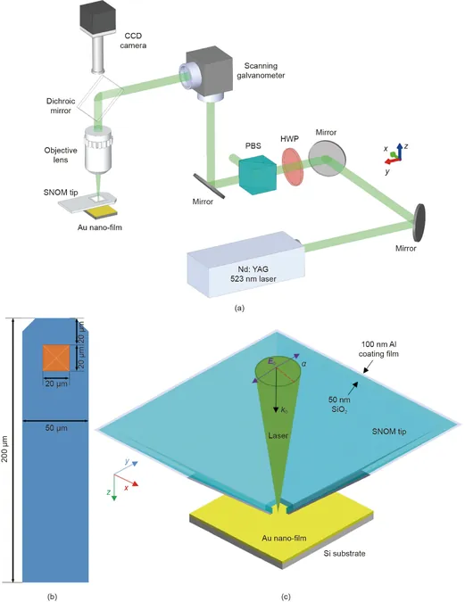
In a groundbreaking study, a research team from Xi'an Jiaotong University, spearheaded by Xuesong Mei and Jianlei Cui, has made significant advancements in the realm of nanotechnology with the successful direct writing of intricate nanostructures on a gold (Au) nano-film. This innovative technique utilizes a nanosecond-laser-irradiated cantilevered scanning near-field optical microscopy (SNOM) probe tip, marking a monumental leap forward in nanofabrication methods.
Background
Nanostructure fabrication has historically faced significant hurdles, particularly due to the diffraction limit that confines conventional optical lithography. Furthermore, electron beam lithography fails to adapt to metal nanofilms, leaving researchers needing more efficient alternatives. The emergence of scanning probe lithography (SPL) provides a promising solution, although each method varies in application conditions.
Innovative Technique
This latest research introduces a revolutionary laser direct-writing system, which consists of a nanosecond laser, specialized optical components, and an atomic force microscope (AFM). Remarkably, this process enables the direct inscription of subwavelength nanostructures on gold nanofilms, eliminating the necessity for masks or a vacuum environment.
Key Findings
According to the findings published in the esteemed journal *Engineering*, the team achieved a remarkable minimum linewidth of just 83.6 nm, with a consistent linewidth of approximately 167.8 ± 6.6 nm on the gold nano-film. The researchers meticulously explored various factors that affect the dimensions of the nanostructures, including single-pulse energy and the polarization angle.
Theoretical Insights
The theoretical calculations illustrated intriguing findings: the elliptical heat distribution beneath the SNOM tip resulted in varying linewidths depending on the scanning orientation. Further investigation through elemental analysis with an energy dispersive spectrometer (EDS) confirmed that the technique relies on melting the Au nanofilm rather than oxidation processes.
Mechanism of Action
This method utilizes locally excited surface plasmon polaritons (SPPs) to create a high-temperature spot under the probe tip, delivering a nanoscale energy source conducive for high-resolution fabrication.
Applications and Implications
Not only does this technology exemplify convenience and cost-effectiveness in nanostructure creation, but it also showcases vast potential applications in nanolithography across various materials, including exciting possibilities in nanowelding techniques.
Future Outlook
As researchers continue to explore the extensive implications of this method, the future of nanotechnology looks brighter than ever! Stay tuned for more updates on this incredible journey into the nanoscale realm that’s set to transform technological landscapes.

 Brasil (PT)
 Canada (EN)
 Chile (ES)
 Česko (CS)
 대한민국 (KO)
 España (ES)
 France (FR)
 Hong Kong (EN)
 Italia (IT)
 日本 (JA)
 Magyarország (HU)
 Norge (NO)
 Polska (PL)
 Schweiz (DE)
 Singapore (EN)
 Sverige (SV)
 Suomi (FI)
 Türkiye (TR)
 الإمارات العربية المتحدة (AR)