Revolutionary Quantum-Controlled Nanoprinting Breakthrough Set to Transform Microelectronics and Biomedicine
2025-04-28
Author: Emily
In an exciting development poised to revolutionize the world of microelectronics, optics, and biomedicine, researchers from Jinan University and the Institute of Chemistry at the Chinese Academy of Sciences have unveiled a groundbreaking nanoprinting technology. This innovative method achieves unmatched precision and efficiency, pushing the boundaries of what’s possible in the field.
The Challenge of Two-Photon Absorption
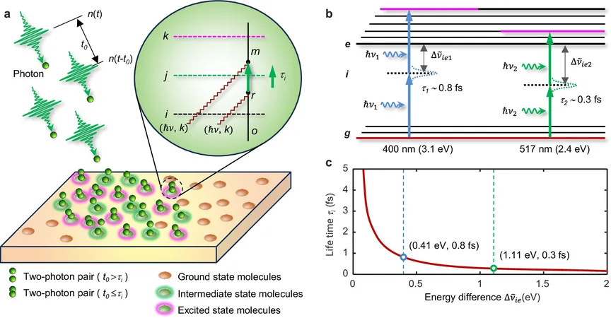
For years, scientists have grappled with the limitations of two-photon absorption (TPA) in optical nanoprinting. The conventional approach has faced a tough dilemma: while increasing light intensity enhances printing speed, it often compromises resolution and can damage sensitive materials. Conversely, a lower intensity maintains resolution but significantly slows down the process, keeping high-performance nanofabrication in a tight spot.
Introducing the Few-Photon Strategy
Now, led by Associate Professor Yuanyuan Zhao and Professor Xuanming Duan from Jinan University, along with Researcher Meiling Zheng's team from the Chinese Academy of Sciences, a revolutionary strategy termed few-photon two-photon absorption (fpTPA) has emerged. This novel technique allows efficient TPA to occur even at extremely low photon exposure, smashing through the long-standing constraints of previous methods.
Harnessing the Power of Light
By meticulously controlling the number of photons in femtosecond laser pulses, the team has unlocked the potential for localized absorption of two photons by a molecule, even under minimalist conditions. Their innovative space-time model delineates the quantum-mechanical interactions at play, pushing the envelope of what optical technology can achieve.
Setting New Records in Resolution
Employing the few-photon approach alongside two-photon digital optical projection lithography (TPDOPL), the researchers have crafted features as tiny as 26 nanometers—an astonishing fraction of the operating wavelength. This achievement represents a dramatic leap over traditional laser writing techniques, enhancing throughput by five orders of magnitude for rapid and high-resolution structure creation.
Novel Techniques for Nanostructure Fabrication
In addition to fpTPA, the researchers introduced in-situ double mask exposure (iDME). This technique allows for the sequential exposure of multiple digital mask patterns, resulting in dense nanostructures with a periodicity of just 210 nanometers—well below the conventional optical limitations without compromising the integrity of the structures.
Versatile Applications Across Multiple Fields
The implications of the few-photon TPA technology stretch far and wide. The research team successfully created diverse micro- and nanostructures, including optical waveguides, microring resonators, and intricate bio-microfluidic channels, demonstrating its potential for optical communication and biomedical engineering. Remarkably, these techniques have also been applied to fabricate microfluidic chips designed for virus detection and cell culture, marking a significant advancement for life sciences.
Accessible Nanomanufacturing for the Future
A vital aspect of this breakthrough is its compatibility with existing optical setups. The few-photon TPA method can be integrated with standard digital optical projection systems, providing a cost-effective and scalable route to cutting-edge nanomanufacturing without necessitating extensive modifications.
A Transformative Leap Forward
"This technology fundamentally changes our approach to two-photon processes," expresses Zhao, highlighting its potential to pave the way for unprecedented advancements in microelectronics, photonics, and biomedicine. With a strong theoretical foundation and expansive application potential, few-photon two-photon absorption is set to reshape the landscape of nanoscale fabrication for years to come.


 Brasil (PT)
 Canada (EN)
 Chile (ES)
 Česko (CS)
 대한민국 (KO)
 España (ES)
 France (FR)
 Hong Kong (EN)
 Italia (IT)
 日本 (JA)
 Magyarország (HU)
 Norge (NO)
 Polska (PL)
 Schweiz (DE)
 Singapore (EN)
 Sverige (SV)
 Suomi (FI)
 Türkiye (TR)
 الإمارات العربية المتحدة (AR)